Semiconductor Vacuum Levels: Why Precision Matters
Semiconductor fabrication operates across an exceptionally wide vacuum spectrum, from atmospheric pressure during wafer loading to ultra-clean high-vacuum environments during critical deposition and etch steps. Typical process pressures include:
- Load-lock and transfer chambers: 1–1000 mbar (rough vacuum for fast cycling)
- Physical vapor deposition (PVD) and chemical vapor deposition (CVD): 10⁻³–10⁻⁶ Torr (medium to high vacuum for uniform film growth)
- Atomic layer deposition (ALD) and plasma etch: 10⁻⁴–10⁻⁷ Torr (high vacuum to minimize contamination and ensure monolayer control)
- End-point detection and leak checking: sub-10⁻⁶ Torr for baseline stability
Even small pressure excursions—±0.01 mbar in rough stages or ±5 % in high vacuum—can cause non-uniform film thickness, particle generation, or yield loss. Real-time, repeatable vacuum monitoring is therefore non-negotiable. Single-gauge solutions fail because no one technology covers the full dynamic range with adequate accuracy and speed. The optimal setup combines complementary sensors that together deliver continuous, gap-free coverage from atmosphere to 10⁻⁷ Torr.
Multi-Gauge Configuration: The Industry Standard
Modern semiconductor tools universally adopt multi-gauge architectures. A rough-vacuum sensor handles pump-down and venting while a high-vacuum sensor takes over once pressure drops below 10⁻³ Torr. Automatic range switching in the tool controller or PLC ensures seamless handover without operator intervention.
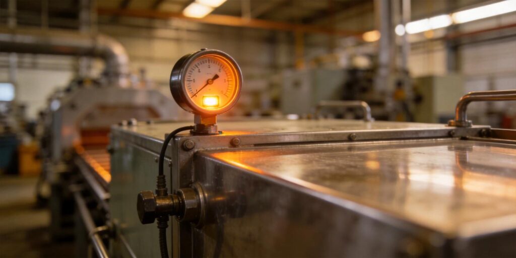
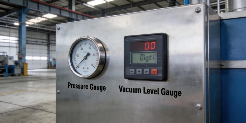
The most cost-effective and compact solution pairs the VG-SP205 Pirani Vacuum Transmitter (atmosphere to 10⁻³ Torr) with the VG-SM225 Cold Cathode Vacuum Gauge (10⁻³ to 10⁻⁷ Torr). Both units share identical RJ45 connectors, 0–10 V analog outputs, and customizable RS232 protocols, allowing a single cable run and unified PLC logic. The combined footprint is significantly smaller than legacy imported pairs, freeing valuable real estate inside crowded cluster-tool cabinets.
This hybrid configuration has become the de-facto standard in new tool designs and retrofits because it eliminates the cost, complexity, and drift issues of wide-range single sensors while providing independent redundancy—critical for 24/7 production environments.
High Vacuum vs. Rough Vacuum: Matching Gauge Technology to the Task
Rough vacuum (atmosphere to 10⁻³ Torr) dominates load-lock cycling, foreline monitoring, and initial pump-down. Here the Pirani principle excels: heat loss from a platinum filament provides fast response (0.5–2 s) and highest accuracy in the linear 10–10⁻² Torr band typical of semiconductor roughing stages. The VG-SP205’s platinum filament offers superior corrosion resistance to residual process gases and requires essentially zero maintenance for 3–5 years.
High vacuum (10⁻³ to 10⁻⁷ Torr) is required for actual deposition and etch. Thermal-conductivity gauges lose sensitivity here; ionization-based cold-cathode technology is mandatory. The VG-SM225 uses a compact positive-magnetron Penning discharge (~100 Gauss NdFeB magnet, –2000 V operating) to sustain a stable ion current down to 10⁻⁷ Torr. Its removable sensor head allows electrode cleaning with 200–500 grit paper in minutes—without breaking chamber vacuum—addressing the contamination common in reactive processes.
| Parameter | VG-SP205 Pirani (Rough) | VG-SM225 Cold Cathode (High) |
|---|---|---|
| Range | Atm to 10⁻³ Torr | 10⁻³ to 10⁻⁷ Torr |
| Linear zone | 10 to 10⁻² Torr | 10⁻³ to 10⁻⁶ Torr |
| Response time | 0.5–2 s | <100 ms |
| Magnetic field | None | ~100 Gauss (compact) |
| Maintenance | Maintenance-free | Field-cleanable head |
Together they cover the entire semiconductor vacuum spectrum with overlapping transition at 10⁻³ Torr, where the cold-cathode software interlock automatically protects electrodes during roughing.
Integration Tips for Semiconductor Tools
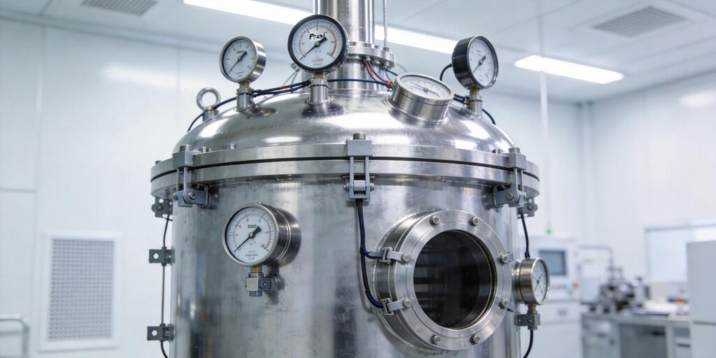
Seamless integration starts with physical mounting. Install both gauges directly on the chamber wall via KF16 or KF25 flanges for true cavity pressure. Use short tube extensions only when thermal isolation is required (e.g., near heated pedestals). The VG-SM225’s arbitrary orientation and compact positive-magnetron design simplify placement even in crowded transfer chambers.
Electrical integration is equally straightforward:
- Analog 0–10 V (effective 2–8 V) connects directly to existing PLC analog inputs for legacy compatibility.
- RS232 digital output with fully customizable protocol (available from 5–10 units) eliminates driver development—define your exact data frame, units, status codes, and polling rate.
- RS485 hardware is pre-reserved on the PCB for future Modbus migration without board changes.
- Route shielded twisted-pair cable at least 10 cm from the cold-cathode magnet and high-voltage lines to minimize noise.
Most semiconductor OEMs implement simple logic: below 10⁻³ Torr the controller ignores the Pirani and trusts the cold cathode; above that threshold the reverse applies. Built-in temperature compensation (15–50 °C) and over-pressure protection on the VG-SM225 ensure stable readings even during rapid thermal cycling.
Compatibility Considerations for Semiconductor Environments
Semiconductor processes introduce unique challenges: complex gas mixtures (Ar, N₂, O₂, reactive precursors), magnetic-sensitive components (electron-beam sources, Hall sensors, precision stages), and strict contamination budgets. Poseidon Scientific’s gauges address these directly.
Gas dependency is managed by factory calibration in air with optional custom mapping for dominant process gases. The cold cathode’s smaller sensitivity variation (typically factor of 2–3 across common gases) complements the Pirani’s stronger thermal-conductivity dependence. Magnetic interference from the VG-SM225’s ~100 Gauss field is minimized by its compact size—maintain 20–30 cm from electron optics or magnetic encoders (or use simple mu-metal shielding). The Pirani contributes zero stray field, making the pair safe for mixed installations.
Material compatibility is assured: stainless-steel electrodes, PEEK insulators, and vacuum-grade seals deliver leak rates ≤10⁻¹¹ Pa·m³/s with negligible outgassing. The VG-SM225’s field-cleanable design prevents cumulative contamination that could otherwise migrate to wafers. Both models have been evaluated in mass-spectrometer and vacuum-heat-treatment lines (initial target markets) and are now under active semiconductor validation for plasma and deposition tools.
Ready to Optimize Your Semiconductor Vacuum Measurement?
The combination of the VG-SP205 Pirani Vacuum Transmitter for rough vacuum and the VG-SM225 Cold Cathode Vacuum Gauge for high vacuum delivers the performance, compactness, and integration flexibility semiconductor equipment builders and end users demand—while cutting costs 30–50 % versus premium imported alternatives. Custom protocol support from just 5–10 units removes integration barriers, and the field-maintainable cold-cathode head reduces downtime to minutes.
Whether you are designing next-generation cluster tools, retrofitting legacy PVD/CVD systems, or scaling ALD capacity, this dual-gauge setup provides continuous, stable vacuum monitoring across the full semiconductor pressure range.
Contact the Poseidon Scientific applications engineering team today for a no-obligation consultation. Provide your chamber geometry, dominant gases, quantity, and integration requirements, and receive a firm quotation, custom protocol sample, and performance recommendation within 24 hours.
Explore full specifications and request an evaluation kit:
Upgrade to the best vacuum gauge setup for semiconductor equipment. Reduce cost, simplify integration, and maximize yield—your optimized solution starts here.